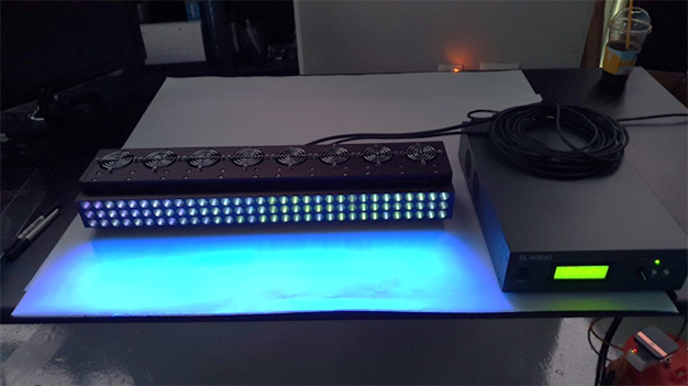
1) Feature : Mainly applied to targeted small-area
2) Resolution : Min 5㎛
| Technical Specifications | ||
|---|---|---|
| Light Source | UV Lamp (Peak 365nm) | |
| Effective Area | Max Φ100 mm | |
| Typical Irradiance | Peak Intensity (mW/Cm²) | |
| Working Distance ( @395nm ) |
120mm | ≥ 100 |
| Uniformity | ± 4% | |
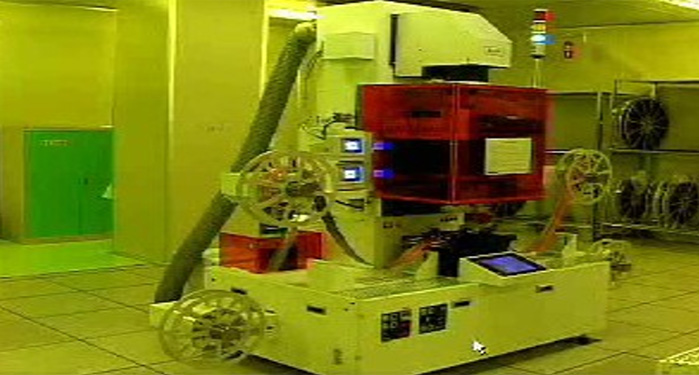
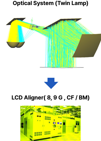
1) Feature : Mostly apply to a large-area exposure unit
2) Resolution : 20 ~ 6 ㎛ (Method: Proximity)
3) Use : LCD, TSP, PDP, PCB
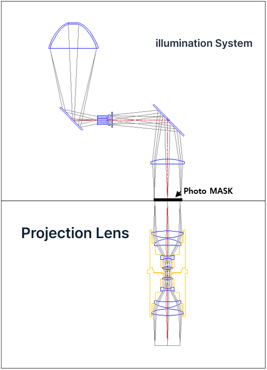
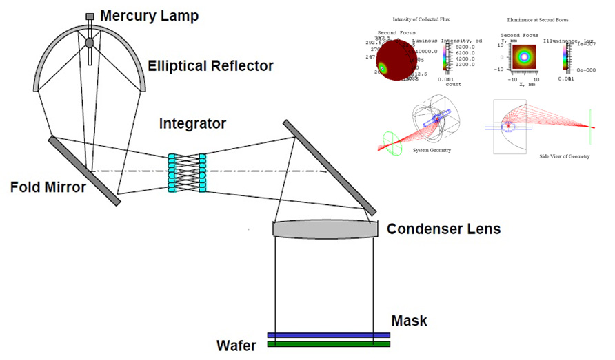
1) Feature : Mainly applied to small-area, high resolution exposure unit. In large area cases, stepper format is applied.
2) Resolution : 20 ~ 3 ㎛ (Method : Proximity) , ~ 0.5 ㎛ (Method: Vacuum Hard Contact)
3) Use : TSP, Semiconductor
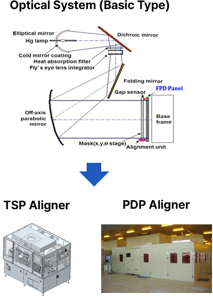
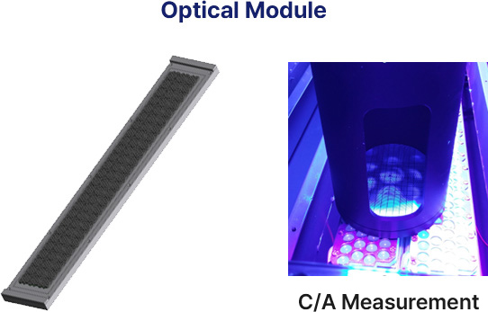
1) Feature : An optical system used in a large-area,
high resolution exposure unit that capable of hard contact. Use UVLED.
By applying a projection lens to each UVLED Chip, C/A (light diffusion angle) can reach at least 2o.
2) Use : PCB, Electronic board
| Technical Specifications | |
|---|---|
| Wavelength | 365/385/395/405nm |
| C/A (Light diffusion half angle) | Min : 2 Degree |
| Scan Uniformity | ≤ ±5% |
* Illuminance and Active area can be changed according to requirements
1) Feature : An optical system used in a super large-area,
high resolution exposure unit that capable of hard contact.
Use UVLED By applying a projection lens to each UVLED Chip, C/A (light diffusion angle) can reach at least 2o.
2) Use : PCB, Other fine pattern production exposure process unit
| Technical Specifications | |
|---|---|
| Wavelength | 365/385/395/405nm |
| C/A (Light diffusion half angle) | Min : 2 Degree |
| Scan Uniformity | ≤ ±5% |
| Beam Area | 60x640 mm |
| Length Availability | Customers Requirements Spec |
* Illuminance and Active area can be changed according to requirements